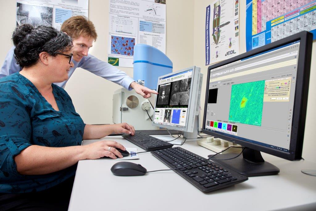
- Lab Services
- Surface Roughness & 3D Topography
- Chemical
- Color Measurement
- Contact Angle
- Gloss Measurement
- Liquids
- Mechanical
- Abrasion
- Contact Stylus Surface Roughness Analysis
- Depth Profiling
- Express Property Mapping through Accelerated Nanoindentation
- Macroscratch
- Microindentation
- Microscratch
- Modulus Mapping
- NanoDMA
- Nanoindentation
- Nanoscratch
- Rheology
- Scratch Testing ISO 1518
- Shore A and Shore D Hardness
- Universal Testing Machine
- Metallurgy
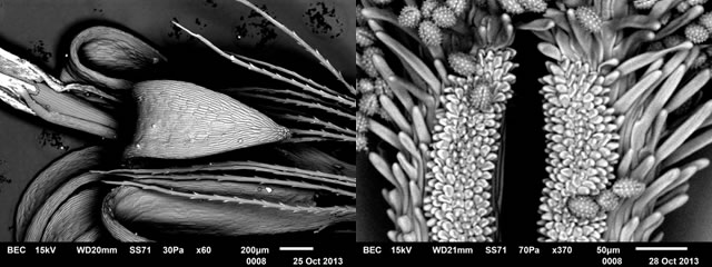
- Microscopy
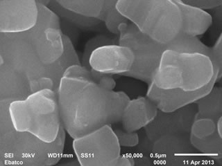
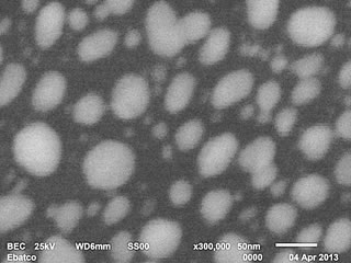
- Particle Size
- Peel Strength
- Pore Size
- Technical Consulting
- Thermal
- Tribological
- X-Ray Diffraction
- Zeta Potential
- Products
- Industries
- Resources
- About Us
- Testimonials
- Contact Us

")