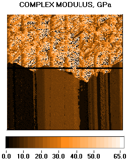
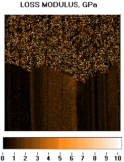
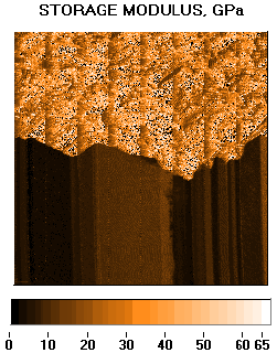
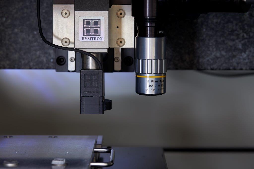
Modulus mapping is a technique to map and display the mechanical properties of a material surface through joint actions of dynamic mechanical testing (nanoDMA) and in-situ SPM (scanning probe microscopy) imaging. A high frequency sinusoidal force is applied to the indenter probe while it is being raster scanned over a sample surface. The resultant displacement of the indenter probe at each pixel position then is analyzed for amplitude and phase lag from the dynamic force input signal. As a result, storage modulus, loss modulus and tangent delta of the material surface are quantified at each pixel position and displayed in a colored image.
Because of the inherited sensitivities of the nanoscale dynamic mechanical testing and scanning probe microscopy incorporated in the technique, modulus mapping has shown promises and advantages in rapidly characterizing and visualizing variation of mechanical properties at nanoscale over grain boundaries, interfaces, inter-phases, multiphase or multilayer composites, precipitates, and additives.

Typical Experimental Results

modulus mappingmodulus mappingmodulus mapping3

Modulus Mapping of Metal-Coating Interface on partially coated wire

modulus mapping

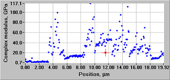
Complex Modulus Line Profile

Applications

Alloys Composite Materials Copolymers
Dynamic Mechanical Analysis Grain Boundaries Heterogeneous Structures
Interfaces Inter-Phases Mechanical Property Mapping
Modulus Mapping Multi-Layers Multi-Phases
Nanomaterials Phase Image Polymer Blend
Precipitates Reinforced Materials Scanning Probe Microscopy
Steels Storage and Loss Modulus Tangent Delta

For more information please read our application notes:

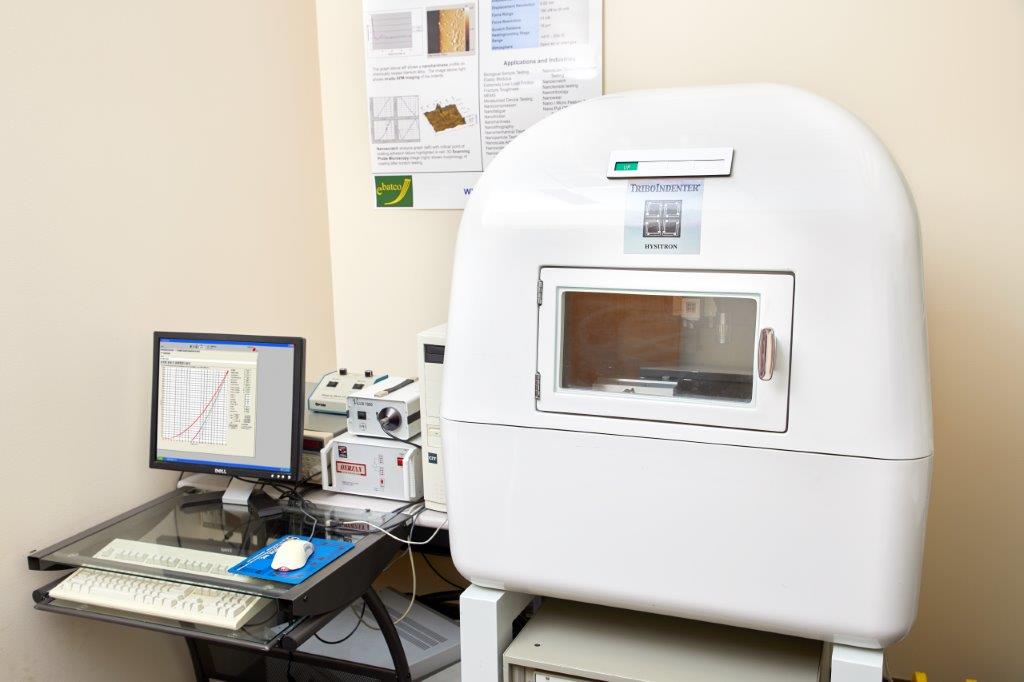
Instrument: Multi-Technique and Full-Feature Nanoindentation System

Key Specifications

Temperature Range 5 to 300 °C
Displacement Resolution 0.02 nm
Force Range 30 nN to 10 mN
Force Resolution 1 nN
Frequency Range 1 to 300 Hz
Atmosphere Open Air, Inert Gas