- Lab Services
- Chemical
- Color Measurement
- Contact Angle
- Gloss Measurement
- Liquids
- Mechanical
- Abrasion
- AFM
- Contact Stylus Surface Roughness Analysis
- Depth Profiling
- Express Property Mapping through Accelerated Nanoindentation
- Macroscratch
- Microindentation
- Microscratch
- Modulus Mapping
- NanoDMA
- Nanoindentation
- Nanoscratch
- Rheology
- Scratch Testing ISO 1518
- Shore A and Shore D Hardness
- Universal Testing Machine
- Metallurgy
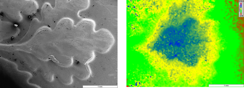
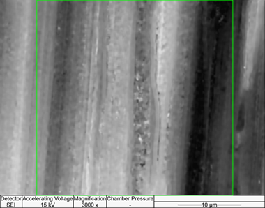
- Microscopy
- Particle Sizing & Counting
- Peel Strength
- Pore Size
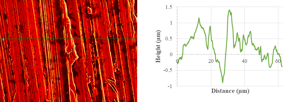
- Surface Roughness & 3D Topography
- Technical Consulting
- Thermal
- Tribological
- X-Ray Diffraction
- Zeta Potential
- Products
- Industries
- Additive Manufacturing
- Aerospace
- Automotive
- Ceramics and Glasses
- Coatings and Thin Films
- Electronics
- Food and Beverages
- Household Products and Cosmetics
- Medical Device
- Metals and Alloys
- Oils and Lubricants
- Packaging and Adhesives
- Pharmaceutical
- Polymers and Composites
- Research and Development
- Semiconductors
- Resources
- About Us
- Testimonials
- Contact Us