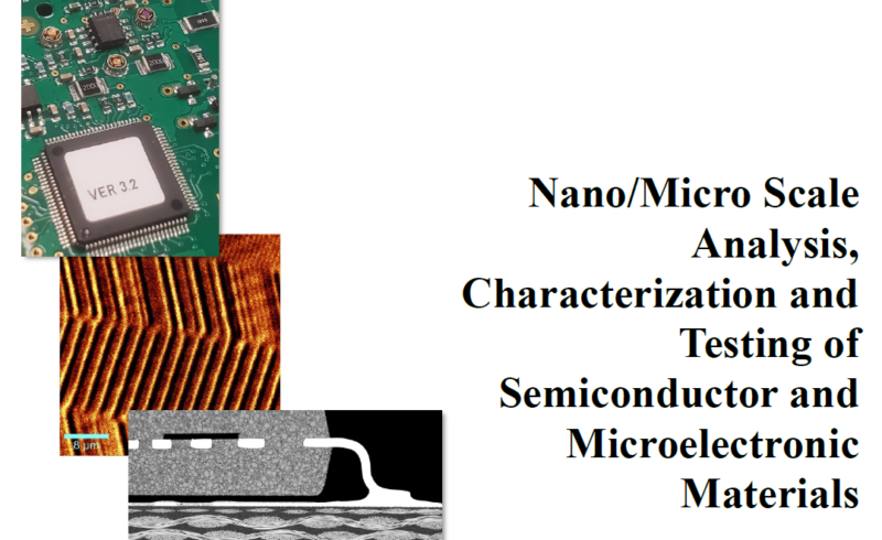
Eden Prairie, MN, April 18, 2024 – Ebatco publishes a white paper on nano/micro scale analysis, characterization and testing of semiconductor and microelectronic materials. Encouraged by the Biden Administration’s CHIPS and Science Act and the booming private semiconductor manufacturing investments, Ebatco, an established and well-recognized lab service power house for nano and microscale materials and device testing, has analyzed the testing needs of semiconductor and microelectronic industries and responded with a suite of contract lab service solutions.
The particular lab services from Ebatco not only claim ISO/IEC 17025:2017 accreditation but also has received admiration and satisfaction feedback from its worldwide customers including many Fortune 500 corporations. Among the lab services, nanomechanical testing (nanoadhesion, nanoindentation, nanocompression, nanoscratch, nanofriction, nanowear) are most popular for ultra-thin film characterizations. Scanning probe microscopy (atomic force microscopy, electrostatic force microscopy, magnetic force microscopy) are great for revealing surface morphology and property distributions. Microscopic contact angle measurements are ideal for wafer surface cleanliness and hydrophobicity/hydrophilicity measurements of micropatterned surfaces. X-ray reflectivity is the best choice for semiconductor surface/interface roughness, film density and thickness measurements. EDS, confocal Raman and FTIR are top selections for unknown chemical identification and distribution mapping. Predominantly, Express Property Mapping (XPM) available through Bruker TI 980 Nanoindenter has gained a significant amount of attention for semiconductor interface mechanical property investigation at sub-micron resolution.
Request a copy here:
Semiconductor and Microelectronic Materials